Production at a glance
Every operation — imaging, drilling, plating, solder mask, testing — happens under one roof in Miroslava, Iași, for a complete, controlled production flow.
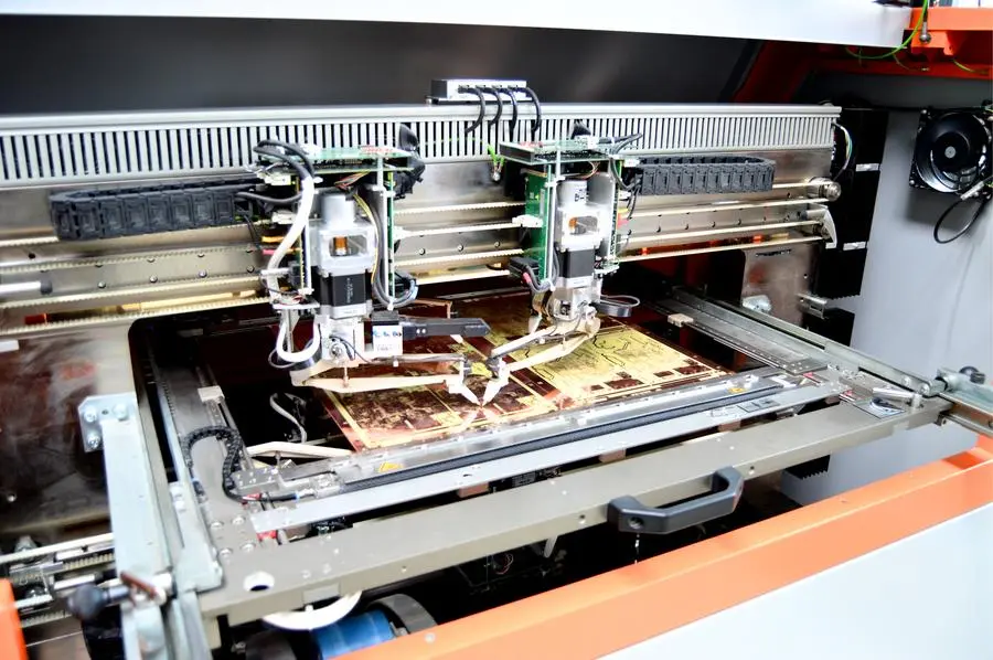
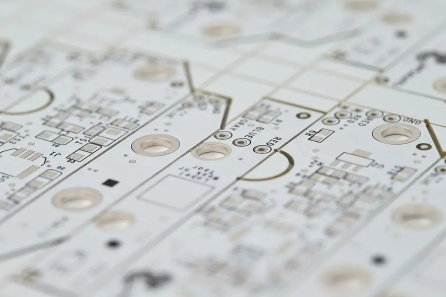
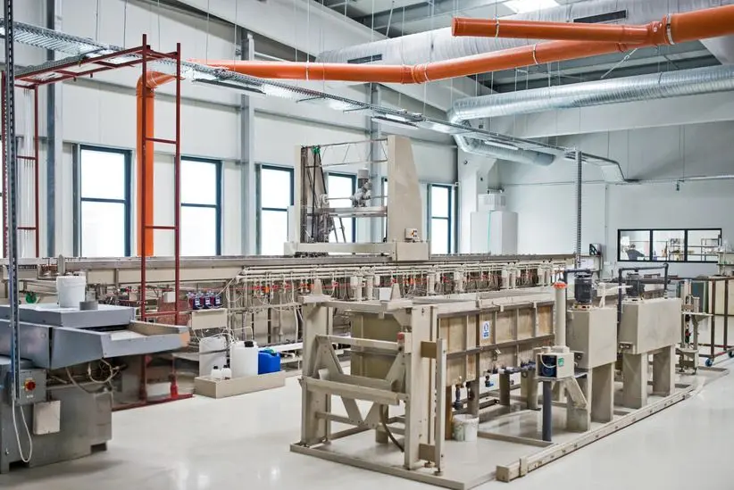
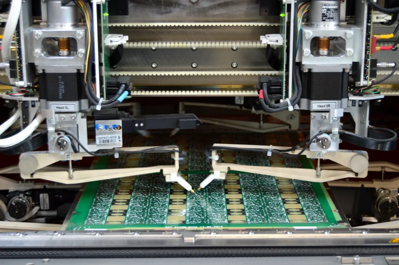
From raw material to finished board, ready for assembly
The complete process every PCB goes through in our facility, from raw laminate to a tested, finished board.
Panel cutting
Panels are cut from the base laminate to the exact working dimensions.
Drilling
Holes for components and vias are drilled per the technical documentation (min. 0.3 mm), then checked for diameter and position.
Carbon deposition (Metallization 1)
Hole walls are cleaned and coated with a conductive carbon layer, creating the conductivity needed for the copper plating step that follows.
Photoresist application
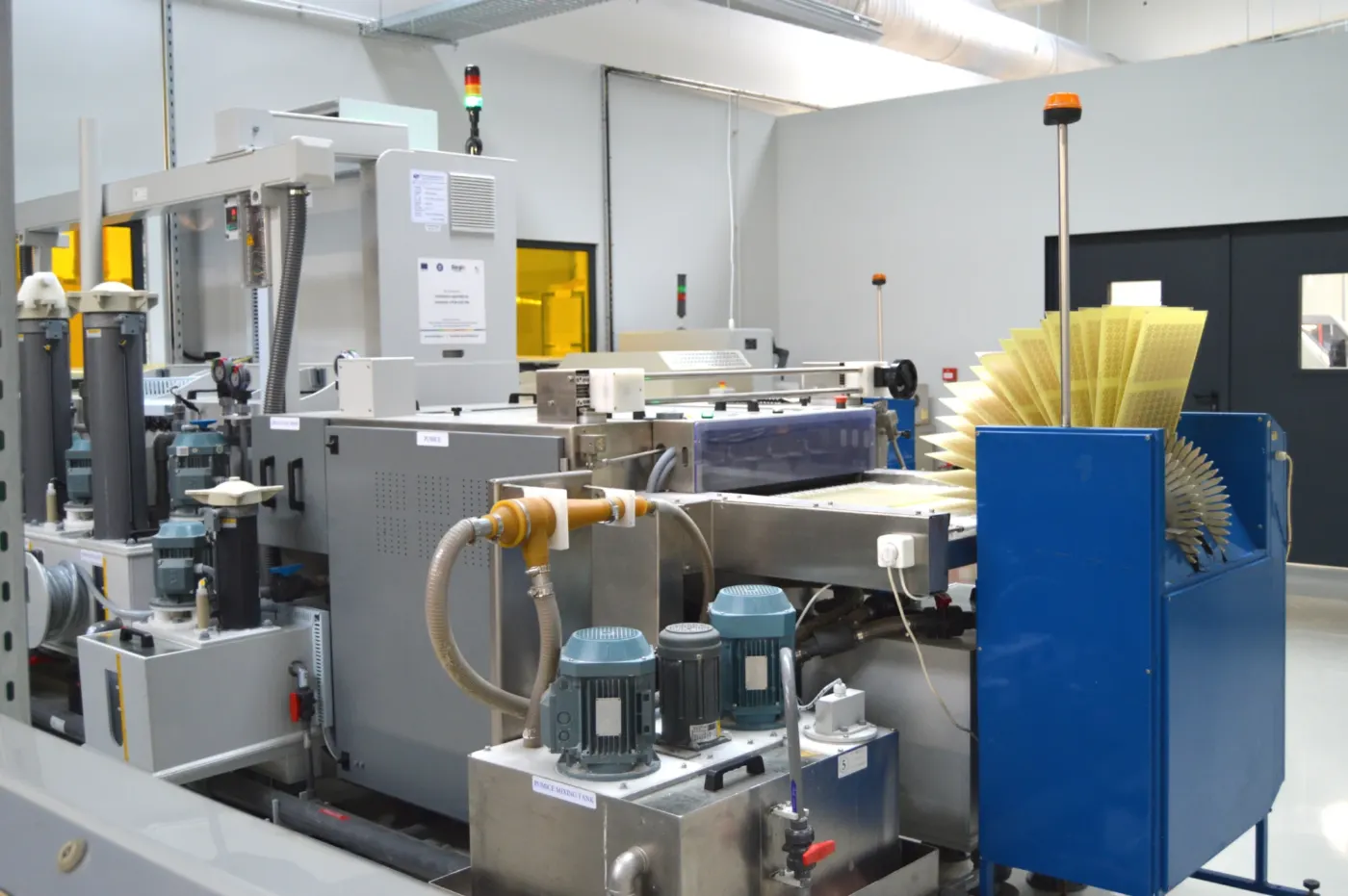
A photoresist film is applied to the panel surface to protect the areas that must be preserved during circuit formation.
Exposure
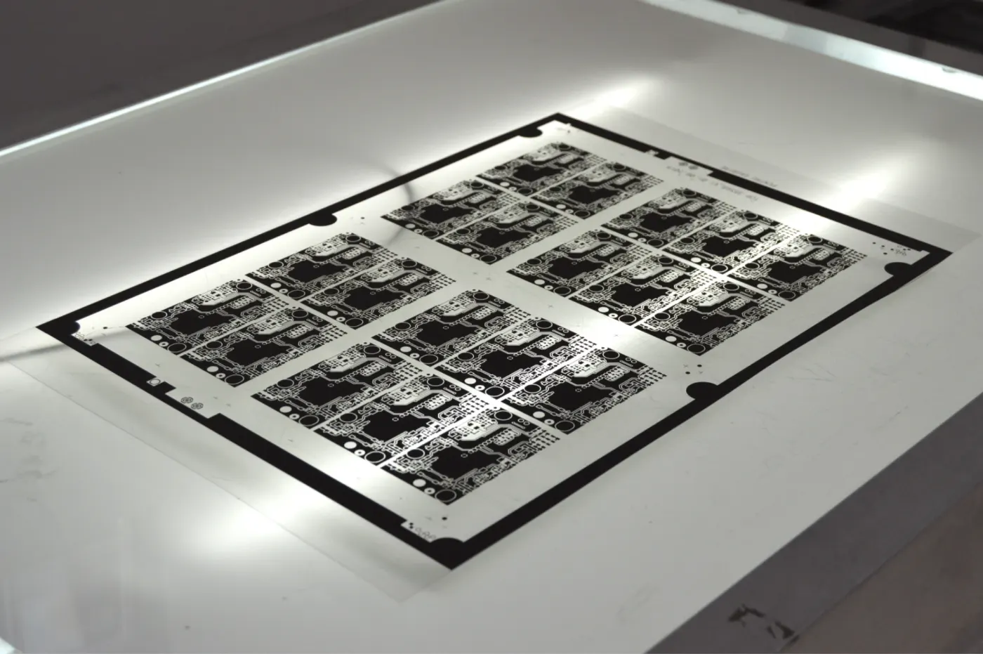
The photoresist is exposed to UV light through a phototool, transferring the circuit image and technological features onto the panel.
Copper plating (Metallization 2)
Copper is electrochemically deposited onto the panel surface and inside the holes, creating the electrical connection between layers.
Stripping
The photoresist is removed after the plating process.
Etching
Unprotected copper is etched away, forming the final electrical traces of the circuit.
AOI inspection
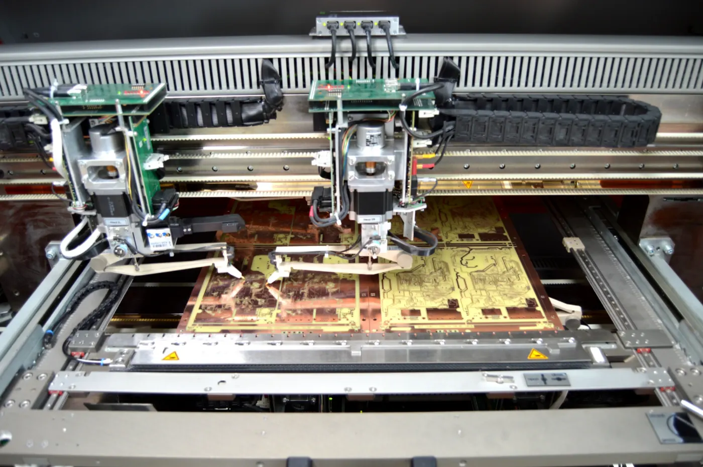
Automated Optical Inspection (before the solder mask) checks traces for breaks, shorts, missing or excess copper and geometry deviations.
Solder mask
The protective solder mask is applied; exposure and development leave the pads and solder areas open.
Silk screen
Component references, polarity marks and other required markings are printed onto the board.
Surface finish
The specified surface finish is applied to the contact pads, protecting the copper and ensuring good solderability.
Electrical test — Open & Short
Every board is electrically tested end-to-end: Open checks for broken connections, Short checks for unwanted connections between nets.
Routing
The final board outline, cutouts and other mechanical features are machined as specified in the drawing.
Sorting
Boards are sorted and separated by test result and by production batch/order.
Final inspection
Visual and dimensional inspection of appearance, outline, holes, silkscreen, solder mask and any remaining defects.
Packaging
Conforming boards are labeled, packaged and prepared for storage or shipping.
Want to know what we can build for you?
See our full capability range — layers, materials, dimensions and finishes.